Recap:
So far we have built chips which can perform many boolean logic operations for us. One of the main chips being the ALU, which will perform a big role in the computer we are going to build.
What we’ve been missing so far:
We have created chips that perform boolean operation for us. However one key thing is that they work on combinatorial logic. What is that? Well essentially it means every desired operation happens at once in a single time unit. (Time unit here refers to a defined length of time eg: 1 micro second). Thinking back to the major problem we faced in the last week. The problem was that we could not operate on data sequentially meaning one after another. Hence the logic we were utilizing was called combinatorial logic.
There is a second type of logic which you might have already guessed is called sequential logic. In sequential we can operate on the same piece of data one after another. But in order to perform such logic operation what we need is the ability to remember the data to be operated on. And that’s where the concepts of memory and time come into play.
First we need to familiarize ourselves with the concepts of time units. In order for chip to perform the desired operations physically it requires time for the electricity to reach the chip, compute and output the result. So we define a universal unit of time (length of time). For example we say a time unit it equal to 1 micro second. Why 1 micro second? Because we can be sure that in that much amount of time the desired operation will be performed by the chips involved. This essentially helps us take care of the issue of time in computers.
Secondly, we move on to memory. Combining our understanding of time in computers. We can now say that purpose of a memory unit it is to reflect data from one time unit into another. This will allow us to perform multiple operations on the same piece of data.
So after this brief theory on time/memory. We can start of focus on the practical implementations of these concepts. In the real world we’ll build some circuits called latches which can be built by combining logic gates we’ve already built. However specifically in Nand2Tetris this concept was sort of overlooked and we were just given a chip called a DFF (Digital Flip Flop). A DFF would output a bit from the previous time unit without much explanation of the circuit being used in it.
But the DFF is not the complete story. Since it simply outputs the bit it receives in the next time unit. But what if we want to output the bit from second last time unit and not from the last time unit? We would need some sort of load operation to direct a chip if we want to hold on to the input data.
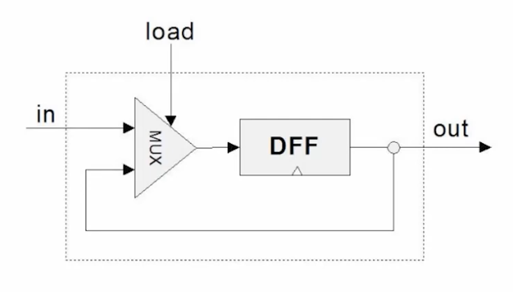
The image above describes how such a chip could be constructed in which we can load some data on demand. Such a chip is called the bit chip in Nand2Tetris. When looking at this image one thing is brand new. That we’re feeding the output of the chip into itself. It’s weird but it can happen and it’ll become important. I heard someone describe it as self-referential logic which makes sense, as we’re doing just that.
Register:
I always used to be afraid to touch low level concepts such as registers. I thought it was like a beast (which I made up in my mind) that required so much to understand. Do you know how a register is made? You just combine the bit chips we created above to whatever size of register we want! It’s just that….
The register’s job is to hold data in itself.
RAM:
So what is a RAM? It’s called Random Access Memory. The name reflect its property which allows us to access any location in the memory at Random. We can decide we can to decide access X and then Y location and it’s possible!
So how is a RAM made? Well it’s very simple actually we just combine a bunch of registers together and we get a RAM chip. Although one new thing required here is the ability to address a location in memory. When working with a register we just need to use a register name. When a lot of registers are combined together we still need a way to send our input to the desired register.
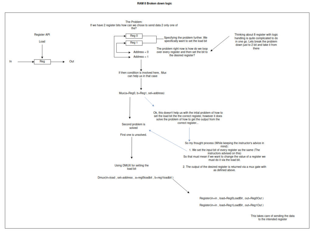
In the spirit of not complicating thing let’s tackle the first problem. We want to combine 8 registers to make a RAM chip. Let’s simplify that with just using 2 registers to understand the concept. A new thing comes into play. That’s the need of address.
An individual register can be utilized anytime by it’s name, however what about when we have them combined together? We will need a way to address registers combined together. This is where the concept of addresses come in where each register has a unique address and we can utilize is it to perform Input/Output operations on a register.
Obviously the address it self will be made up of bits. So first thing we need to figure out is how many bits should be utilized given n number of registers for their addresses?
In order to optimally create unique addresses for every register present on the RAM we can apply the formula k = log2(n). Where n = The number of registers. k will represent number of bits required to create a unique addresses for every register. This takes care of the addresses.
Now after understanding the concept of addresses. We need to think about the practical implementation. Let’s get the easy part out of the way first. Whatever input is being fed into the RAM will be fed into every register. We can do that because only until the load bit is set will the register load in the input. So we just need to figure out how to set the correct load bit on a register? I had to brain storm this a little. However after some thought, a D-MUX gate offers us just that functionality. Here’s a Virtual Board I used while brain storming in-case you’re interested:
Onto expanding the RAM. Once again it’s very simple. Just stack a bunch of smaller RAMs together and handle the addressing via multiplexers so the input reaches the desired destination.
PC:
One of the most critical components to construct the CPU is the PC (Program Counter). Program counter represents what instruction should be executed next. It’s used to control the flow of execution.
Think of when you use an if statement in your code? When the condition is true the code execution flows changes. Thinking about this function in a low level to get it done we need a component like PC. Which will actually dictate where the next instruction is which we can manipulate via some code. For instance when an if condition is evaluated.
The PC is also a register — A special kind of register. It can remember data and transmit it from one time unit to anothe
But it’s additional functionality includes the ability for us to manipulate it to change its states in predictable ways.
For example we will have 4 input pins each for their own specific purpose:
- Input
- Load
- Reset
- Inc
Input:
Just like a regular input pin of a register it feeds a 16 bit input number into the register.
Load:
Again like a regular load bit for a register. When the load bit is one register will load the input bits into itself.
Reset:
This is where things get interesting. When the reset bit is asserted, we want the register to be set to the value 0.
Inc:
Inc stands for increment. When this bit is asserted we want the register to add 1 to it’s current value.
Now the next question that comes to mind is: What operation should have precedence over another. For example: If Inc and Reset asserted should the output be 0 or 1?
The Nand2Tetris IDE offers a great way to experience the PC chip, so you can experiment around with it and understand such caveats. So after playing around with the chip in IDE I was able to understand that the Order of precedence should look something like this:
- Reset
- Load
- Inc
After this observation one concept was left which was crucial for building the PC chip: self-referential logic. Remember how earlier it was mentioned that HDL is not sequential? Meaning everything happens all at once. Well taking advantage of that, we can accomplish something interesting. Essentially, we can put the output of a chip as it’s input as well.
At first it seems trippy but it’s fantastic! This concept is more well understood when constructing latches such as the AND-OR or the SR latche. Latches are the building blocks for the DFF, but since we were handed a DFF in the course we didn’t walk through their underlying functionality.
After understanding these fundamental concepts. It should be relatively easy to construct the PC chip. As at the end of the day it’s just a register with some extra functionality.
Conclusion:
Well, that’s another week finished! I still find it fascinating that computers are so so simple. I now understand how this stuff works and it was just that simple. There isn’t any rocket science. It’s just plain logic true and false. There are lots of logic gates acting while I press these keys to type. A physical change is occurring as I press these keys electrons are moving the memory map for the screen is getting updated to display these characters in real-time. How amazing is that? Under all this complexity are some humble logic gates doing our bidding.